The following work was provided by Keegan Ryan, an NCC Group consultant.
This past January, I ordered a new TV. Since I was concerned about how an Internet-connected TV has the potential to be hacked, I wanted the simplest device I could find. I didn’t need anything fancy: no Internet connectivity, no downloadable apps, just something that could display an HDMI signal on a screen. This simple requirement still necessitates significant complexity under the hood, so I bought the TV with the expectation that the device would still have a powerful processor running complicated firmware. Once the device arrived, this eventually led to the question of whether it would be possible to put Spectre on the TV. A couple weeks ago, I decided to try.
But probably not in the way you’re thinking.
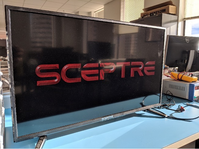
The TV was manufactured by Sceptre Inc. (note the ‘C’ and ‘P’ switch) and was covered in SCEPTRE branding. My goal for this project was to perform a hardware-level attack against the TV and change the branding to SPECTRE as an homage to the microarchitectural attack. This project has nothing to do with exploiting speculative execution, but instead it demonstrates several common techniques NCC Group uses when analyzing embedded systems.
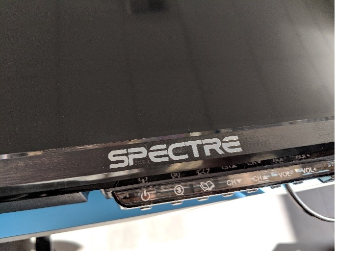
There are two prominent locations on the TV where I want to change the branding. The first is the silver logo at the bottom of the frame, and the second is the large SCEPTRE splash screen as the TV turns on.
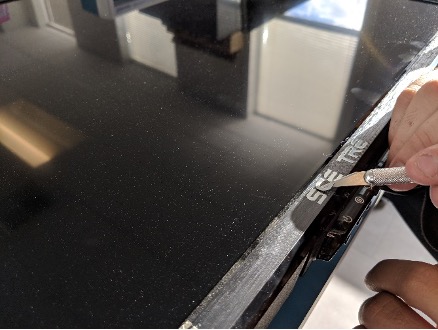
The first modification is quite easy. Each letter in the silver logo is a single sticker, so it’s easy to peel up the ‘C’ and the ‘P’, swap them, and leave the other letters unmodified.
The second modification will take considerably more work, but based on our experience with similar hardware engagements in the past, it should be fairly straightforward. The data representing the SCEPTRE logo must be somewhere on the device, so I expect the image to reside on either a microcontroller or flash chip within the TV. Since this is a cheap TV which doesn’t hold any sensitive data, there probably aren’t many hardware security features I need to bypass. Finally, I expect the splash screen data to be stored in an easily-parsed format, since it’s frequently faster to read an uncompressed image directly from memory than wait for more sophisticated loading code to run. If I can modify the uncompressed data, it will be easy to swap the bytes corresponding to the ‘C’ and ‘P.’
There are three steps to this modification. First, disassemble the TV and understand where the logo data might be stored. Second, read off that data and find the offset and format of the splash screen. Third, edit the image and rewrite the data to the TV so the modified logo is displayed as the TV turns on.
Disassembly and Reverse Engineering
After unplugging the TV, we start by removing the back panel and observing the layout of the circuit board.
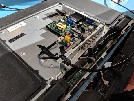
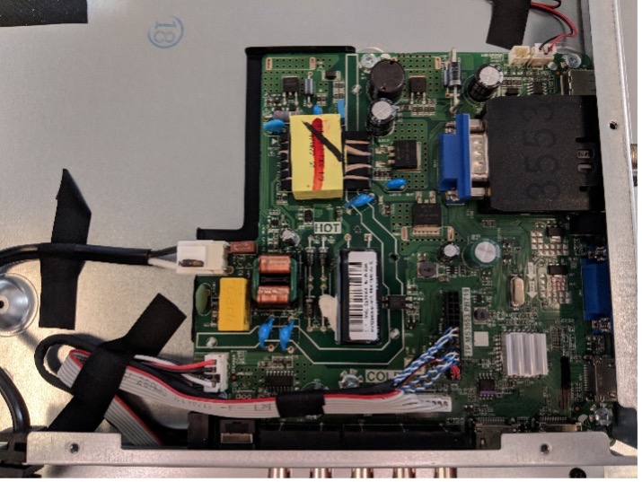
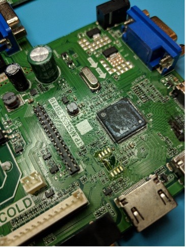
The top left of the board, labelled “HOT,” contains a large transformer and capacitor and is electrically isolated from the “COLD” side of the board with a thick channel, so this is where AC power from the outlet is converted to DC for the components on the board. There are exposed leads on the hot side of the board, so we need to be careful when feeding power to the board for testing. The lower left corner contains connectors leading to the speakers, LED screen, and buttons, and the top right contains various connectors for video input. So far, there isn’t anything that might contain the splash screen data.
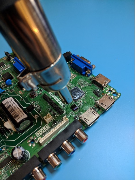
However, the lower right corner of the board contains an 8-pin chip with a stripe of purple paint and another chip with a heat sink. The 8-pin form factor is common for SPI flash memory chips, and paint marks are often used to mark memory after it has been programmed, so there’s a good chance that this chip contains some sort of data. The heat sink is likely used to cool the board’s main System on a Chip (SoC), which handles the majority of the logic on the device, so with the mechanical assistance of some vise grip pliers, I remove the heat sink and scrape away the thermal compound to read off the part numbers.
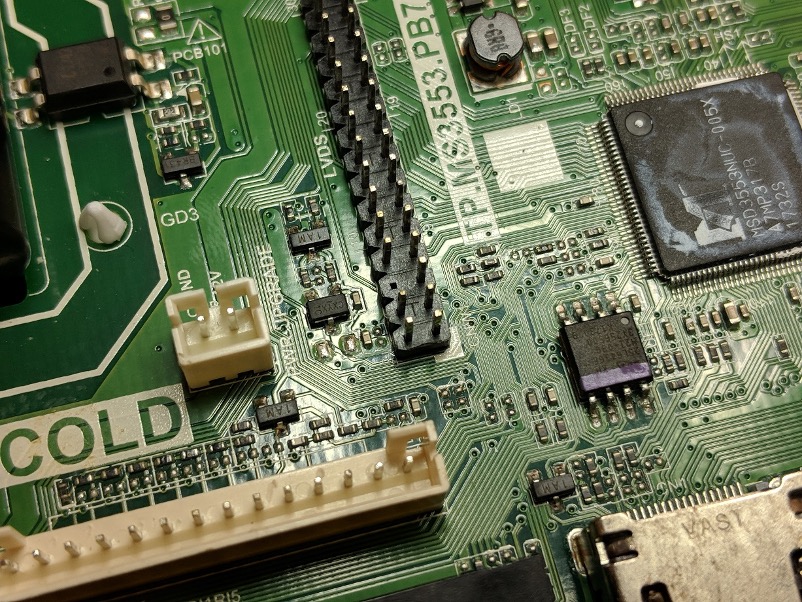
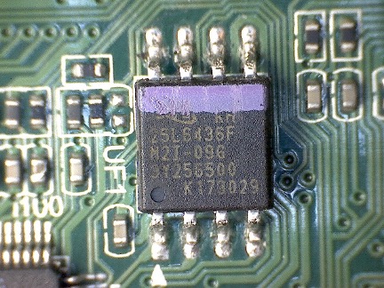
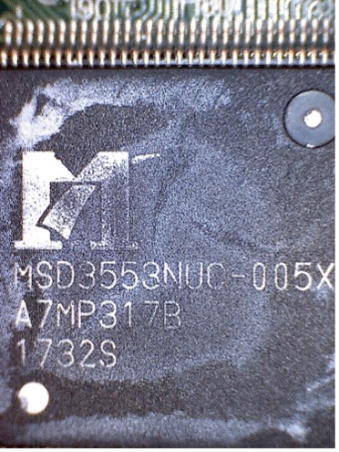
The first is indeed a SPI flash chip from Macronix, which according to the datasheet has 3.3V voltage levels and 8 megabytes of storage capacity. The second is a high-speed processor from MStar which includes HDMI and programming ports and various audio and video decoders, so this is definitely the main SoC on the board.
Reading the Memory
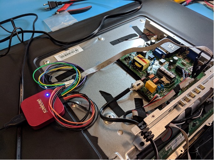
Now that I know where the flash memory is, the next step is recovering the data from the chip. There are many ways to do this, so I prefer to start with the least invasive. Frequently, when a SPI flash chip and SoC appear so close to one another, the flash is used to store firmware for the SoC. In this scenario, the SoC often sends SPI read commands to load the entire flash into RAM as it boots, and monitoring voltage levels on the SPI bus for a few seconds is sufficient to recover the memory contents. I connect a Saleae logic analyzer to the flash chip using a test clip and start capturing.
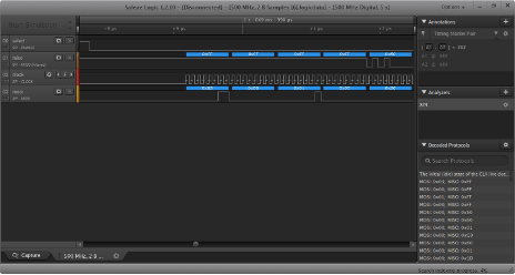
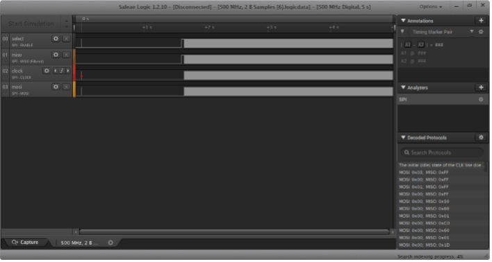
The good news is that as soon as the device boots, the SoC sends read commands (hex 03 and hex 0B) to the flash chip, and the flash chip responds with valid data (starting with hex 50). The bad news is that the SoC only accesses a few kilobytes of the 8 total megabytes and shows no sign of reading the rest of flash within the first few seconds.
This is a good start, but I need to try something else to retrieve the flash contents. If I can send my own SPI read commands directly to the flash chip, I can access the full 8 megabytes without waiting for the SoC. On some boards, it’s possible to send these commands while the flash chip is still on the powered-down board, but this is not always the case. I’ve had issues in the past where I can’t power the flash chip without inadvertently powering other components on the board, preventing a clear signal. Unfortunately, that is the case here, so I’ll have to remove the flash chip from the board in order to send my own SPI commands. A hot air rework station makes quick work of that task.
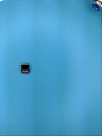
Once desoldered, there are a few different devices that can be used to read the flash. One example is the FlashCat with the test clip from earlier, but this time I opt for a BusPirate and DIP8 socket adapter.
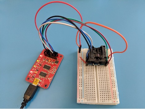
With this setup, I send the corresponding SPI commands to read all 8 Mb of flash memory and reconstruct the flash image. Now it’s time to start analyzing this image in search of the splash screen.
Running strings on the binary file quickly confirms that we have valid data:
$ strings -n 30 flash.bin | head
oversubscribed literal/length tree
incomplete literal/length tree
oversubscribed dynamic bit lengths tree
incomplete dynamic bit lengths tree
too many length or distance symbols
[Whisky] DDR2 BondSW10 Error!!!
!!!Acquire Send Mutex for SWI2C Failed!
FFFFFFFF[PM_WHISKY] Enter Standby Loop
MDrv_DVI_Set_SWCK_ByPort(u8DviPortIdx=%u, bEnable=%u)
[PM_WHISKY] Console Initial OK
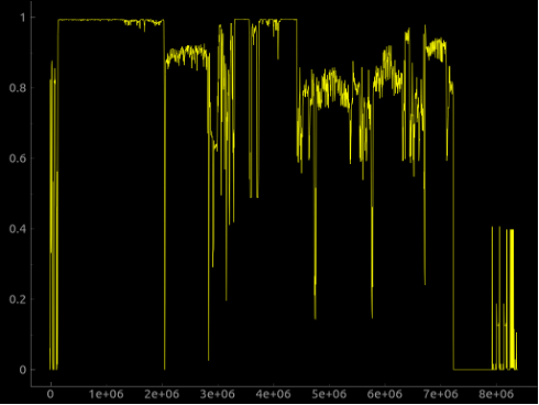
In particular, these human-readable strings indicate that there might be a debugging interface or UART console which I could use in case it’s too difficult to understand the flash image statically. Next, the entropy analysis of binwalkreveals a few high-entropy compressed or possibly encrypted regions, some lower-entropy regions which might correspond to machine code, and some zero-entropy regions corresponding to unused space.
The real magic happens when we use binwalk to scan for common file signatures:
$ binwalk flash.bin
DECIMAL HEXADECIMAL DESCRIPTION
——————————————————————————–
106472 0x19FE8 Unix path: /whisky/pm/core/interrupt.c
106621 0x1A07D Unix path: /whisky/pm/core/timer_cb.c
2886942 0x2C0D1E MySQL MISAM index file Version 10
2886998 0x2C0D56 MySQL MISAM index file Version 7
2887988 0x2C1134 MySQL MISAM index file Version 1
2889631 0x2C179F MySQL MISAM index file Version 1
2899473 0x2C3E11 MySQL ISAM index file Version 9
2905225 0x2C5489 MySQL MISAM index file Version 1
2907207 0x2C5C47 MySQL MISAM index file Version 4
2907726 0x2C5E4E MySQL ISAM index file Version 5
2912349 0x2C705D MySQL ISAM index file Version 2
2915244 0x2C7BAC MySQL MISAM index file Version 3
3577176 0x369558 JPEG image data, EXIF standard
3577188 0x369564 TIFF image data, big-endian, offset of first image directory: 8
3584549 0x36B225 Unix path: /www.w3.org/1999/02/22-rdf-syntax-ns#”>
Right there, sitting at offset 0x369558, is a JPEG image. I use dd to copy it out of the firmware file, open it up, and I am greeted with this:
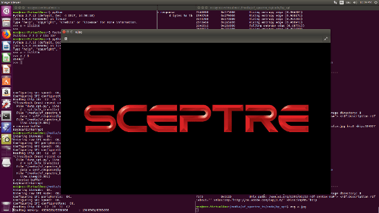
Success! Now that I’ve recovered the splash screen from the flash chip, all I have to do now is modify it and write it back.
Modifying the TV
JPEG images are a compressed format, so unfortunately, I can’t just swap raw bytes around to exchange the ‘C’ and ‘P.’ I can, however, load the JPEG into GIMP, make the swap, and save the resulting file as a new JPEG.
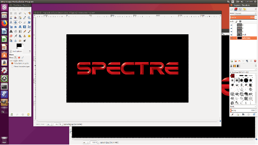
Luckily, the new JPEG is smaller than the old one, so I can just modify the firmware image at the same 0x369558 offset as before without worrying about overwriting the data after the original JPEG. Hopefully the JPEG decoder in the TV will not care about the change in file length and happily display the altered data.
Having created the newly modified firmware image, I now need to write the image back to flash memory and reconnect the reprogrammed flash chip to the TV. The first part is easy, since I can just use the BusPirate or FlashCat to send the correct SPI write commands. For the second part, I could just resolder the flash chip in place, but I don’t know if I modified the firmware correctly yet. I might need to update a checksum in the flash to account for the modified data, or maybe I need my JPEG to be exactly the same length as the original. If I resolder the flash chip now, I might have to go back and desolder it again to fix any mistakes. Instead, I solder a few wires where the flash chip is supposed to go and connect them to the test clip from earlier.
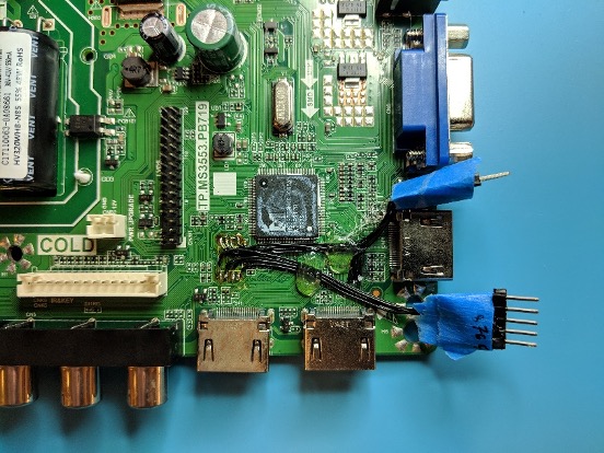
Now I can replace the heat sink, reassemble the TV, and have an easy way to connect or disconnect the flash chip from the system.
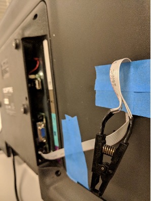
I send the write commands, attach the flash via the test clip, power the TV on, and… nothing. The splash screen still says SCEPTRE. How could this be? I detach the chip, reread its contents, and find that the data at the end of the address space has changed, but the splash screen JPEG is unchanged from its original value.
Clearly, it must be possible to write to the chip because some of the memory has changed, but when I try to modify the splash screen, the contents stay the same. There must be something else in place on this flash chip that prevents modification of this region. I read through the datasheet, and sure enough, there are configurable block protection bits. These are used to prevent accidental modification of certain memory regions, so I quickly modify my BusPirate script to disable the protection bits, reflash the memory using the FlashCat, and re-enable the protection bits just to be safe.
I put the newly reflashed chip back in the test clip, power the TV on, and success!
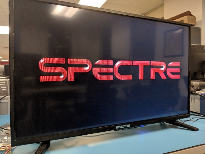
In the end, overwriting the JPEG in the flash memory was all I needed to do to replace the splash screen. Having confirmed the modification worked, I remove the test clip, resolder the flash chip, and put everything back together.Since the modifications I made require physical access and don’t obtain sensitive information, this research is in no way represents a security flaw in the device, but rather this was a fun exercise in understanding an unknown system. Although I was successful in changing the silver logo and the splash screen, there are still some interesting areas that could be explored some more. The flash image could be reverse engineered further, particularly the high-entropy compressed sections at the beginning. A few of the menus still have the original SCEPTRE logo, so the data backing these could be identified and changed as well. There are also probably debugging and UART interfaces on the device, and finding these would give even greater insight into the operation of the SoC. However, I achieved what I was after, so I’ll leave further exploration along these paths to future research. For now, I’m satisfied with being greeted by a side channel every time I turn on the TV.
