Vendor: NXP Semiconductors
Vendor URL: https://www.nxp.com
Affected Devices: i.MX RT 101x, i.MX RT102x, i.MX RT1050/6x, i.MX 6 Family, i.MX 7 Family, i.MX8M Quad/Mini, Vybrid
Author: Jon Szymaniak
CVE: CVE-2022-45163
Advisory URL: https://community.nxp.com/t5/Known-Limitations-and-Guidelines/SDP-Read-Bypass-CVE-2022-45163/ta-p/1553565
Risk: 5.3 (CVSS:3.0/AV:P/AC:L/PR:N/UI:N/S:C/C:H/I:N/A:N), 2.6 if C:L, 0.0 if C:N
Summary
NXP System-on-a-Chip (SoC) fuse configurations with the SDP READ_REGISTER operation disabled (SDP_READ_DISABLE=1) but other serial download functionality still enabled (SDP_DISABLE=0) can be abused to read memory contents in warm and cold boot attack scenarios. In lieu of an enabled SDP READ_REGISTER operation, an attacker can use a series of timed SDP WRITE_DCD commands to execute DCD CHECK_DATA operations, for which USB control transfer response times can be observed to deduce the 1 or 0 state of each successively tested bit within the targeted memory range.
Location
The affected code is located within the immutable read-only memory (ROM) used to bootstrap NXP i.MX Application Processors; it is not customer-updatable.
Impact
Any confidential assets stored in the DDR memory or non-volatile memory mapped registers (e.g. general purpose fuses) associated with the affected chipset could be more easily retrieved by an attacker with physical access to a target device.
The level of effort required to extract memory contents from affected systems without HABv4 enabled (i.e. an “open” device) may be greatly reduced, depending on the accessibility of the SDP interface. Instead of performing memory extraction through execution of malicious firmware, built-in ROM functionality can be abused.
When HABv4 is enabled (i.e. a “closed” device) NCC Group observed a limiting factor — only one DCD could be executed per boot. The attack is still theoretically possible but requires significantly more overhead between each bit-read attempt to reset or power cycle the target; the data extraction rate becomes limited by how quickly the USB SDP interface can enumerate.
Details
NXP i.MX system-on-a-chip (SoC) devices provide a variety of security features and eFuse-based configuration options that customers can choose to enable, according to their threat model and security requirements. In systems leveraging HABv4 in a “closed” or “secure boot” configuration, software images booted via the UART or USB OTG-based Serial Download Protocol (SDP) must still pass cryptographic signature verification.
For this reason (and based upon NCC Group’s observations during security assessments), some NXP customers may opt to leave the Serial Download Protocol (SDP) boot mode enabled in order to initially bootstrap platforms during manufacturing and/or to execute diagnostic tests. (Although highly discouraged, many do not actually enable HAB due to project schedule limitations or other factors.) Such customers may use the SDP_READ_DISABLE fuse to prevent the SDP READ_REGISTER operation from being abused by a malicious party seeking to extract sensitive information from device memory in either a warm or cold boot attack.
The types of assets regarded as sensitive and requiring strong confidentiality guarantees is expected to vary based upon a variety of factors, including the product markets of NXP’s customers and security expectations of end-users. Examples include, but are not necessarily limited to:
- Application or protocol-layer authentication tokens
- Cryptographic key material (not stored in dedicated hardware-backed key storage)
- DRM or product license information
- Personally identifiable information (PII) and end-user data including:
- Location
- Device usage history
- Stored or cached multimedia captures
- Financial or payment card data
- Trade secrets or other sensitive intellectual property
The boot images supported by NXP i.MX processors may contain “Device Configuration Data” (DCD) sequences, consisting of a limited set of operations (see i.MX6ULLRM Rev 1, 8.7.2 Device Configuration Data). Common use-cases of DCD functionality include clock initialization, configuration of I/O interfaces needed to retrieve a boot loader, and DDR memory controller configuration. For example, DCD functionality can alleviate the need to use multiple boot stages to overcome internal SRAM size limitations; a larger U-Boot “proper” image can be booted directly from NAND instead of requiring a U-Boot SPL to first be executed from internal SRAM to configure DDR for use by the successive U-Boot stage. Oftentimes, an NXP customer can re-use the DCD settings provided in open source reference designs with few, if any, changes.
When a device boot fails, or is otherwise specifically forced, into its Serial Download Protocol (SDP) boot mode, the SDP WRITE_DCD command can be used to send a DCD to a target device to execute. Below is a sequence diagram illustrating the series of HID reports involved in performing the SDP WRITE_DCD operation. Observe that Report3 is sent by the target device upon completion of DCD execution. Note that the value tresp represents the turnaround time from the host sending its final Report2 and the time at which it receives the Report3 response from the target device. texec is the amount of time that the target is actually executing the DCD. The latter is not directly observable, but the former can be treated an estimate of the DCD execution time, with some added overhead.
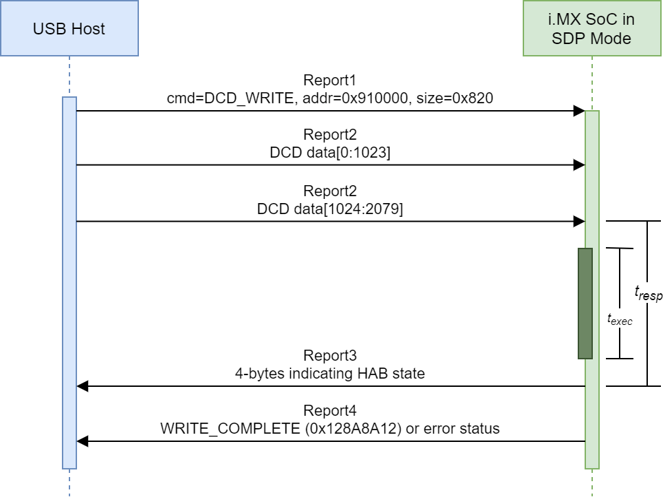
The DCD CHECK_DATA command can be used to instruct the boot ROM to read a 32-bit value at a specified address and evaluate an expression with it. The expression is defined by “mask” and “set” parameters shown in the following table.

An optional 32-bit count parameter allows this command to be used to repeatedly poll a register until one or more bits are in the desired state. An example use case might be polling “PLL locked” status bits before proceeding to further configure peripheral subsystems.
If the expression is true then the boot ROM moves onto the next operation in the DCD. Otherwise, it will perform upwards of count iterations of the test. If the iteration limit is reached, the boot ROM will move onto the next command. This operation is effectively a no-op (NOP) when a count value of zero is specified. Without a count value, the boot ROM will poll indefinitely. For further clarity, this behavior is described in the following code excerpt.
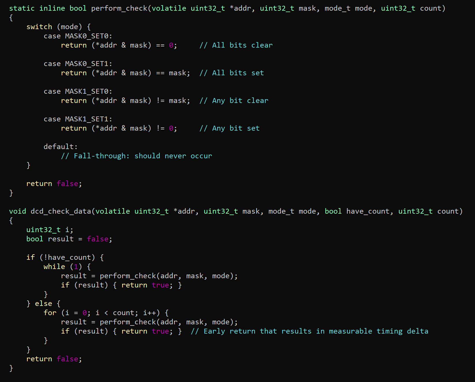
To summarize:
- The
countparameter is attacker controlled, included in an SDP request - texec can be approximated by timing a Report3 response frame
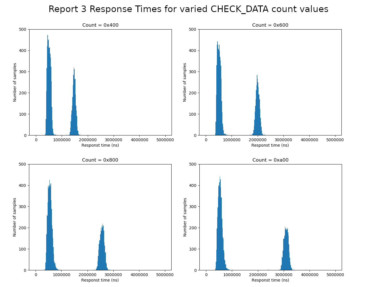
- The time value can be used to deduce if a bit tested via CHECK_DATA was a 1 or 0.
The behavior describe above allows CHECK_DATA to be abused as an arbitrary memory read primitive, albeit a slow one. This is the case regardless of the SDP_READ_DISABLE=1 fuse setting which disallows use of the SDP READ_DATA command, and therefore represents a violation of the intended security policy. Because data stored in DDR memory decays relatively slowly (as opposed to SRAM) when its controller is no longer performing refresh cycles, an attacker may be able to recover desired data on already powered off devices (see Halderman et al.).
Leveraging CHECK_DATA as a DDR memory read primitive, NCC Group collected timing samples for a sweep of different count parameter values on an i.MX6ULL development kit. The bimodal nature of data, shown below, indicates the feasibility of the attack for well-chosen count values. The following section summarizes a proof of concept, remarks on results, and discusses the practicality of leveraging this in an attack.
Proof of Concept
In order to evaluate the practicality of an attack, NCC Group developed an internal tool called “imemx” to perform memory readout on SDP-enabled NXP i.MX devices, supporting both the standard READ_REGISTER operation and the aforementioned timing side-channel. Given the nature of the vulnerability and the challenges of patching it, we will not be releasing this tool publicly.
Instead, the remainder of this section outlines the high-level process we followed to confirm the vulnerability and evaluate the effectiveness of its exploitation. Note that the degree of difficulty (or lack thereof) associated with each step largely depends upon factors resulting from design, board layout, and manufacturing decisions made by the NXP customer.
Step 1: Induce Loading of Target Data into Memory
Depending upon the target system, certain (target-specific) actions may need to be performed before assets of interest are decrypted, received, or otherwise loaded into RAM. A few examples for different types of products are presented below.
- Powering the device on and waiting short period of time for runtime initialization procedures to complete.
- Performing basic user interaction with the device
- Waiting for the device to receive a configuration update via its LTE interface.
- Pairing the device with a companion mobile application via Bluetooth.
- Producing sensor stimuli that results in MQTT events being sent to a backend system.
To simplify verification, we wrote a known random pattern to the first few kilobytes of the target address from within the U-Boot boot loader using commands such as mw and loadb.
Step 2: Force Device into SDP Mode
Next, the target device must be forced into its SDP mode of operation. If the device has not been configured with “Boot from Fuses” setting, this can be achieved by asserting BOOT_MODE[1:0]=0b10 on associated I/O pins during a warm or power-on reset. Otherwise, it is necessary to temporarily induce non-volatile storage access failures during to cause the target device to fail into the SDP boot mode (similar to failing open into a U-Boot console in example 1 or example 2).
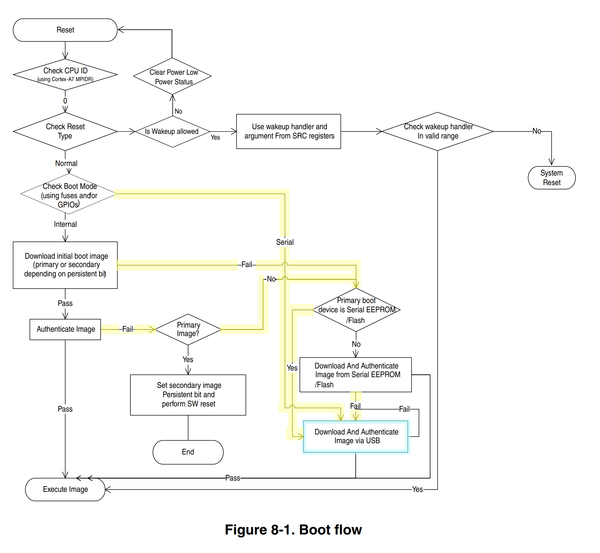
For convenience, Figure 8-1 from the i.MX6ULL Reference Manual (i.MX6ULLRM ) is reproduced below. Observe that the SDP boot mode is reachable via multiple highlighted flows, including the “boot from fuses” setting.
Step 3: Initialize DDR Controller via DCD
In order to perform a warm or cold boot attack on a device, one must first perform any initialization required to interface with the DDR memory. Typically, this is implemented via DCD or in a U-Boot SPL. For the purposes of this proof-of-concept, we assume the requisite configuration parameters have already been extracted from another device’s non-volatile storage or over-the-air update file. Also note that it may still be possible to leverage information from open source implementations or third-party reference designs that a product was derived from to produce usable DDR configurations in the well-documented DCD format.
Once a DCD containing sufficient initialization has been prepared (a priori), it can be written to the device using NXP’s Universal Update Utility (UUU):
$ uuu SDP: dcd -f ./target_config.imx
uuu (Universal Update Utility) for nxp imx chips -- libuuu_1.4.107-15-gd1c466c

Success 0    Failure 0

3:41     1/ 1 [============100%============] SDP: dcd -f ./target_config.imx
Okay
Care must be taken to not send a DDR configuration to the device more than once; doing so was observed to lock up the target. On HAB-enabed devices, only one DCD can be sent per boot. This implies that this step and the following step must be combined, with the DCD containing both the actual target configuration and the CHECK_DATA read primitive. As a result, a larger count value was required (due to the added DCD execution overhead) and only 1 bit per boot could be achieved on HAB-enabled devices. (Our experiment tooling automatically power-cycled the target after each bit-read.)
Step 4: Execute CHECK_DATA-based Memory Readout Attack
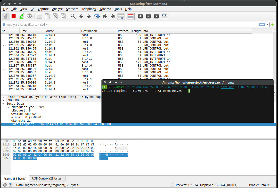
Finally, the CHECK_DATA timing side-channel can be exploited. The following invocation reads a 4KiB region of memory, bit-by-bit, starting at address 0x82000000. The window threshold parameters establish which timing values to consider a 0 or a 1. Our tool performs retries of any ambiguous results, up to a configurable maximum retry limit.
$ ./imemx -t -t-win-low 75000 -t-win-high 90000 -t-count 0x800
               -o data.bin -a 0x82000000 -s 4k

98.88% complete   51.26 B/s    ETA: 00:00:00.90
---------------------------------------
Completed in 1m19.901131805s
# Retries: 91
The following screenshot shows imemx running while Wireshark monitors the associated USB HID traffic.
Step 5: Analysis
The resulting data can then be analyzed to locate items of interest. For test purposes, vbindiff was used to compare the input test data with the data back from the device. Some bit-errors are expected due to the slow degradation of DDR contents – the degree of error is expected to increase with the amount of time since the device was powered off. An excessive number of errors may suggest that more appropriate time thresholds for bit value determination should have been chosen.
In reality, the (non) triviality of this depends upon the target. API keys and session tokens in HTTP traffic may be conspicuous by virtue of their printable representation. Sensitive data in well-known file formats (e.g. private key in SSLeay format) may be retrieved by simply running binwalk on the memory dump. Other scenarios, however, may require a more complex constraint-driven approach that leverage a priori knowledge (or inferences) about data structure layouts in order to make productive use of tools such as Volatility. Rather than attempting to extract all of DDR memory, a more efficient approach may be to read only as much memory required to identify per-task kernel data structures, and then leverage these to further deduce the location of active memory mappings.
Conclusions
The limited data rate and expectation of random bit-errors limit the effectiveness of this attack to scenarios in which an attacker would have prolonged access to a device they own, have found, or have stolen. Ultimately, the value (and lifetime) of potential assets would dictate whether or not a time investment of hours, days, or even weeks constitute a worthwhile effort. In some situations, this may simply represent an attack that can be run “in the background” while developing and testing a custom OCCAM-resident firmware image to achieve the same result.
Recommendations
NCC Group recommends that affected NXP customers revisit the threat models of their own customers and products and take the following steps, if it is determined that:
- Prolonged physical access to (lost, stolen) devices is plausible
AND - Sensitive assets or confidential data may reside in DDR RAM
Mitigations
- Disable SDP in production devices by setting the SDP_DISABLE eFuse bit to 1.
- If available, also set UART Serial Download Disable eFuse bit to 1.
- As a matter of security best practice, and especially for NXP devices without CAAM support (e.g. i.MX6ULL), seek to limit the lifetime of sensitive assets (e.g. key material) in memory, immediately overwriting memory locations with zeros or randomized patterns when these assets are no longer immediately needed by software.
- If self-test or diagnostic functionality is required, implement this via an authenticated diagnostic unlock mechanism (pgs 20-23) in the first non-ROM bootloader stage.
- If significantly privileged access is required to support failure analysis, with analyzed devices not being returned to the field, consider using HAB authenticated bootloader functionality and using the FIELD_RETURN fuse mechanism to perform a permanent return to an “insecure” diagnostic state.
- If not doing so already, leverage the CAAM on supported chipsets for cryptographic operations, such that secrets such as key material is neither accessible to software executing on the device, nor ever stored in DDR memory.
- Although still vulnerable, enabling HAB appears to introduce an additional (data throughput) barrier to practical exploitation. If doing so is feasible, the use of authenticated boot functionality is encouraged.
While obscuring access to the SDP interface signals through PCB routing strategies or application of tamper-resistant potting or encapsulation compounds is not regarded by NCC Group as a solution, these approaches can impede efforts to exploit the vulnerability documented here. When performing cost-benefit analyses for remediation efforts, an accurate threat model should first be created and reviewed in order to assess the plausibility of threats and the effectiveness of applied mitigations.
Vendor Communication
2022-08-18 – Draft advisory submitted to NXP PSIRT for coordinated disclosure.
2022-08-18 – NXP PSIRT acknowledges receipt of advisory.
2022-08-23 – NXP PSIRT indicates analysis of report and proof-of-concept are ongoing.
2022-08-31 – NXP confirms NCC Group’s finding of a novel attack and concurs with disabling SDP as being a viable mitigation. NXP PSIRT indicates other affected devices and mitigations are currently being evaluated.
2022-09-13 – NXP provides status update indicating additional time is required to complete product portfolio analysis and communicate with affected customers.
2022-09-14 – NCC Group extends disclosure deadline by 30 days to accommodate the above.
2022-09-30 – NXP PSIRT provides status update.
2022-10-14 – NXP PSIRT provides status update and requests additional time to communicate with affected customers.
2022-10-14 – NCC Group extends disclosure deadline to Nov. 17th, 2022.
2022-11-11 - NXP PSIRT provides status update and indicates CVE-2022-45163 has been reserved.
2022-11-14 - NCC Group acknowledges receipt of information.
2022-11-15 - NCC Group sends update regarding upcoming publication.
2022-11-17 - NCC Group publishes advisory.
Acknowledgements
Thank you to Jeremy Boone, Jennifer Fernick, and Rob Wood for their always-appreciated, invaluable guidance and support. Additional gratitude is extended to NXP PSIRT for their responsiveness throughout the disclosure process.
About NCC Group
NCC Group is a global expert in cybersecurity and risk mitigation, working with businesses to protect their brand, value and reputation against the ever-evolving threat landscape. With our knowledge, experience and global footprint, we are best placed to help businesses identify, assess, mitigate respond to the risks they face. We are passionate about making the Internet safer and revolutionizing the way in which organizations think about cybersecurity. NCC Group Hardware and Embedded Systems Services leverages decades of real-world engineering experience to provide pragmatic guidance on architecture and design, component selection, and manufacturing.
